

IBM Research announced today that it has built the first functional 7-nanometer test chips, in collaboration with GlobalFoundries, Samsung and SUNY Polytechnic Institute's Colleges of Nanoscale Science and Engineering.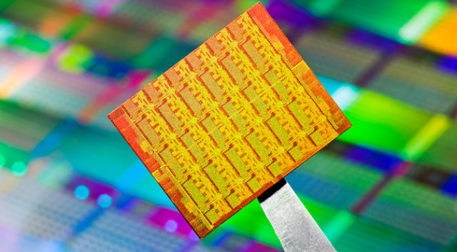
The company hopes that the new processors it is currently testing will be the beginning of the smallest semiconductors available, and that new semiconductor technology will continue to shrink upcoming products for at least two to three years.
To put that into perspective, a 7nm node is a little bigger than human DNA, which is 2.5nm in diameter. Processors today range from 10nm, 14nm, and 22nm in size.
IBM's new generation of chips is expected to deliver new innovations that will power the company's products, including its Watson supercomputers as well as its cloud and data center mainframes.
According to IBM, the 7nm test chip was created using silicon germanium (SiGe) transistors and Extreme Ultraviolet (EUV) lithography.
IBM plans to invest $3 billion over five years in chip research and development, so we're probably going to see some amazing things.
On July 1, IBM closed the deal to sell its microelectronics business to Globalfoundries, which acquires the intellectual property, production capacity and employees.
Globalfoundries is the former manufacturing company of AMD, and the largest private semiconductor manufacturing company.
